Developed to analyze new semiconductors, the system could streamline the development of more powerful solar panels.
Scientists are striving to discover new semiconductor materials that could boost the efficiency of solar cells and other electronics. But the pace of innovation is bottlenecked by the speed at which researchers can manually measure important material properties.
A fully autonomous robotic system developed by MIT researchers could speed things up.
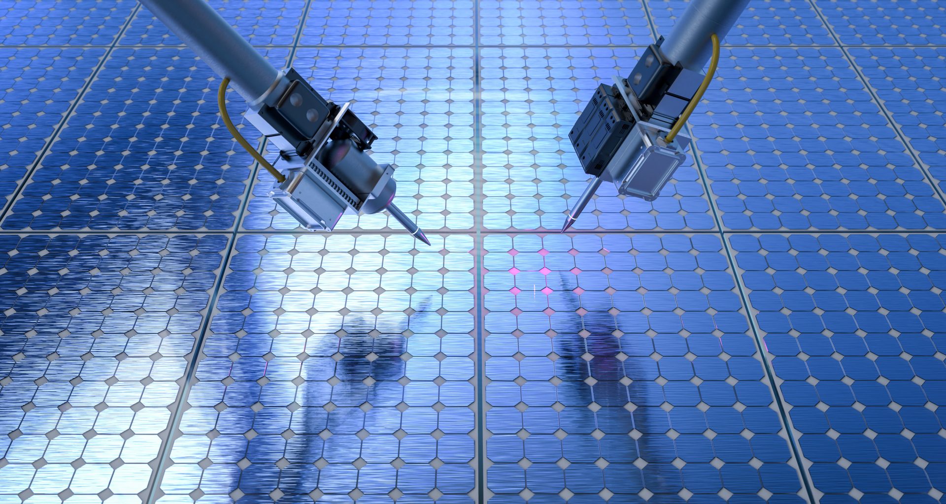
Their system utilizes a robotic probe to measure an important electrical property known as photoconductance, which is how electrically responsive a material is to the presence of light.
The researchers inject materials-science-domain knowledge from human experts into the machine-learning model that guides the robot’s decision making. This enables the robot to identify the best places to contact a material with the probe to gain the most information about its photoconductance, while a specialized planning procedure finds the fastest way to move between contact points.
During a 24-hour test, the fully autonomous robotic probe took more than 125 unique measurements per hour, with more precision and reliability than other artificial intelligence-based methods.
By dramatically increasing the speed at which scientists can characterize important properties of new semiconductor materials, this method could spur the development of solar panels that produce more electricity.
“I find this paper to be incredibly exciting because it provides a pathway for autonomous, contact-based characterization methods. Not every important property of a material can be measured in a contactless way. If you need to make contact with your sample, you want it to be fast and you want to maximize the amount of information that you gain,” says Tonio Buonassisi, professor of mechanical engineering and senior author of a paper on the autonomous system.
His co-authors include lead author Alexander (Aleks) Siemenn, a graduate student; postdocs Basita Das and Kangyu Ji; and graduate student Fang Sheng. The work appears today in Science Advances.
Making contact
Since 2018, researchers in Buonassisi’s laboratory have been working toward a fully autonomous materials discovery laboratory. They’ve recently focused on discovering new perovskites, which are a class of semiconductor materials used in photovoltaics like solar panels.
In prior work, they developed techniques to rapidly synthesize and print unique combinations of perovskite material. They also designed imaging-based methods to determine some important material properties.
But photoconductance is most accurately characterized by placing a probe onto the material, shining a light, and measuring the electrical response.
“To allow our experimental laboratory to operate as quickly and accurately as possible, we had to come up with a solution that would produce the best measurements while minimizing the time it takes to run the whole procedure,” says Siemenn.
Doing so required the integration of machine learning, robotics, and material science into one autonomous system.
To begin, the robotic system uses its onboard camera to take an image of a slide with perovskite material printed on it.
Then it uses computer vision to cut that image into segments, which are fed into a neural network model that has been specially designed to incorporate domain expertise from chemists and materials scientists.
“These robots can improve the repeatability and precision of our operations, but it is important to still have a human in the loop. If we don’t have a good way to implement the rich knowledge from these chemical experts into our robots, we are not going to be able to discover new materials,” Siemenn adds.
The model uses this domain knowledge to determine the optimal points for the probe to contact based on the shape of the sample and its material composition. These contact points are fed into a path planner that finds the most efficient way for the probe to reach all points.
The adaptability of this machine-learning approach is especially important because the printed samples have unique shapes, from circular drops to jellybean-like structures.
“It is almost like measuring snowflakes — it is difficult to get two that are identical,” Buonassisi says.
Once the path planner finds the shortest path, it sends signals to the robot’s motors, which manipulate the probe and take measurements at each contact point in rapid succession.
Key to the speed of this approach is the self-supervised nature of the neural network model. The model determines optimal contact points directly on a sample image — without the need for labeled training data.
The researchers also accelerated the system by enhancing the path planning procedure. They found that adding a small amount of noise, or randomness, to the algorithm helped it find the shortest path.
“As we progress in this age of autonomous labs, you really do need all three of these expertise — hardware building, software, and an understanding of materials science — coming together into the same team to be able to innovate quickly. And that is part of the secret sauce here,” Buonassisi says.
Rich data, rapid results
Once they had built the system from the ground up, the researchers tested each component. Their results showed that the neural network model found better contact points with less computation time than seven other AI-based methods. In addition, the path planning algorithm consistently found shorter path plans than other methods.
When they put all the pieces together to conduct a 24-hour fully autonomous experiment, the robotic system conducted more than 3,000 unique photoconductance measurements at a rate exceeding 125 per hour.
In addition, the level of detail provided by this precise measurement approach enabled the researchers to identify hotspots with higher photoconductance as well as areas of material degradation.
“Being able to gather such rich data that can be captured at such fast rates, without the need for human guidance, starts to open up doors to be able to discover and develop new high-performance semiconductors, especially for sustainability applications like solar panels,” Siemenn says.
The researchers want to continue building on this robotic system as they strive to create a fully autonomous lab for materials discovery.
This work is supported, in part, by First Solar, Eni through the MIT Energy Initiative, MathWorks, the University of Toronto’s Acceleration Consortium, the U.S. Department of Energy, and the U.S. National Science Foundation.